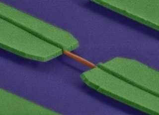
Very tiny wires made of semiconducting material i.e. more than thousand times thinner than a human hair—promise to be an essential component for the semiconductor industry.
Thanks to these tiny nanostructures, scientists envision not only a more powerful new generation of transistors, but also to integrate optical communication systems within the very same piece of silicon, making possible to transfer data between chips at the speed of light.
But for optical communication to happen, it is essential to convert the electrical information used in the microprocessor into light, by using the light emitters. On the other end of the optical link,one needs to translate the information contained in the stream of light into electrical signals by using light detectors. Current technologies use different materials to realize these two distinct functions—silicon or germanium for light detection and materials combining elements from the III-V columns of the periodic table for light emission. However, this might be going to change soon thanks to a new discovery.
In paper appearing today in the journalNature Communications, scientists at IBM Research – Zurich and the Norwegian Univ. of Science and Technology have demonstrated for the first time that both, efficient light emission and detection functionalities can be achieved in the very same nanowire material by applying mechanical strain.Using this new physical phenomenon, scientists might be able to integrate the light emitter and the detector functions in the very same material. This would drastically reduce the complexity of future silicon nanophotonic chips.IBM scientist Giorgio Signorello explains, “When you pull the nanowire along its length, the nanowire is in a state that we call “direct bandgap” and it can emit light very efficiently; when instead you compress the length of the wire, its electronic properties change and the material stops emitting light. We call this state as “pseudo-direct”: the III-V material behaves similarly to silicon or germanium and becomes a good light detector.”IBM Fellow Heike Riel comments, “These are unique and surprising properties and they all come from the fact that the atoms are located at very special positions within the nanowire. We call this crystal structure “Wurtzite”. This structure is possible only because the nanowire dimensions are so small. You cannot achieve thesame properties at dimensions visible to the eye.This is a great example of the power of nanotechnology.”This remarkable properties might find interesting applications also outside the field of optical communication.Inducing a Direct-to-Pseudodirect Bandgap Transition in Wurtzite GaAs Nanowires with Uniaxial Stress
The Tech Portal is published by Blue Box Media Private Limited. Our investors have no influence over our reporting. Read our full Ownership and Funding Disclosure →


