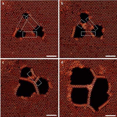


Junhao Lin, a Vanderbilt Univ. graduate student and visiting scientist at Oak Ridge National Laboratory (ORNL), has found a new way to use a finely focused beam of electrons to create some of the smallest wires ever made.
The flexible metallic wires are only three atoms wide i.e. One thousandth the width of the microscopic wires used to connect the transistors in today’s integrated circuits.
Lin’s achievement is described in an article published online in the Nature Nanotechnology. According to his advisor Sokrates Pantelides, a prof. of physics and engineering at Vanderbilt Univ., and his collaborators at ORNL, the technique represents an exciting new way to manipulate matter at the nanoscale and should give a boost to efforts to create electronic circuits out of atomic monolayers, the thinnest possible form factor for solid objects.
“Junhao took this project and really ran with it,” said Pantelides.
Lin made the tiny wires from a special family of semiconducting materials that naturally form monolayers. These materials, called transition-metal dichalcogenides (TMDCs), are made by combining the metals molybdenum or tungsten with either sulfur or selenium. The best-known member of the family is molybdenum disulfide, a common mineral that is used as a solid lubricant.
Atomic monolayers are the object of considerable scientific interest these days because they tend to have a number of remarkable qualities, such as exceptional strength and flexibility with transparency and high electron mobility. This interest was sparked in 2004 by the discovery of an easy way to create a graphene, an atomic-scale honeycomb lattice of carbon atoms that has exhibited a number of record-breaking properties, including strength, electricity and heat conduction. Despite graphene’s superlative properties, experts have had trouble converting them into useful devices, a process materials scientists call functionalization. So researchers have turned to other monolayer materials like the TMDCs.
Other research groups have already created functioning transistors and flash memory gates out of TMDC materials. So the discovery of how to make wires provides the means for interconnecting these basic elements. Next to the transistors, wiring is one of the most important parts of an integrated circuit. Although today’s integrated circuits (chips) are the size of a thumbnail, they contain more than 20 miles of copper wiring.
“This will likely stimulate a huge research interest in monolayer circuit design,” Lin said. “Because this technique uses electron irradiation, it can in principle be applicable to any kind of electron-based instrument, such as electron-beam lithography.”
One of the intriguing properties of monolayer circuitry is it`s toughness and flexibility. It is too early to predict what kinds of applications it will produce, but “If you let your imagination go, you can envision tablets and television displays that are as thin as a sheet of paper that you can roll up and stuff in your pocket or purse,” Pantelides commented.
In addition, Lin envisions that the new technique could make it possible to create the three-dimensional circuits by stacking monolayers “like Lego blocks” and using electron beams to fabricate the wires that connect the stacked layers.